

| Place of Origin: | China |
|---|---|
| Brand Name: | KAZ |
| Certification: | UL&ROHS |
| Model Number: | KAZA-100 |
| Minimum Order Quantity: | 1 Unit |
|---|---|
| Packaging Details: | vacuum package |
| Delivery Time: | 3-14 days |
| Payment Terms: | T/T, Western Union, MoneyGram, L/C, D/A |
| Supply Ability: | 2000 m2 / Month |
| Layer Count: | 2 ` 30 Layers | Max Board Size: | 600 Mm X 1200 Mm |
|---|---|---|---|
| Base Material For PCB: | FR4, CEM-1, TACONIC, Aluminium, High Tg Material, High Frequence ROGERS ,TEFLON, ARLON, Halogen-free Material | Rang Of Finish Baords Thickness: | 0.21-7.0mm |
| Minimum Line Width: | 3mil (0.075mm) | Minimum Line Space: | 3mil (0.075mm) |
| Minimum Hole Diameter: | 0.10 Mm | E-Testing: | 100% E-Testing (High Voltage Testing); Flying Probe Testing |
| High Light: | 30L FR4 SMT PCB Assembly, SMT PCB Assembly 7.0mm Thickness, Lead Free HASL Pcb Prototype Board | ||
Ultrafast PCB fabrication manufacturer, offering one-stop PCB manufacturing, PCB assembly, SMT stencil,cheap and good quality pcb smt assembly
1. Features
1. One Stop OEM Service, PCB manufacturing Made in Shenzhen of China
2. Manufactured by Gerber File and BOM List from Customer
3. FR4 Material, Meet 94V0 standard
4. SMT, DIP technology suport
5. Lead Free HASL, Environmental Protection
6. UL, CE, ROHS Compliant
7. Shipping By DHL,UPS, TNT, EMS or Customer requirement
2. PCB Technical capability
| SMT | Position accuracy:20 um |
| Components size:0.4×0.2mm(01005) —130×79mm,Flip-CHIP,QFP,BGA,POP | |
| Max. component height::25mm | |
| Max. PCB size:680×500mm | |
| Min. PCB size:no limited | |
| PCB thickness:0.3 to 6mm | |
| PCB weight:3KG | |
| Wave-Solder | Max. PCB width:450mm |
| Min. PCB width: no limited | |
| Component height:Top 120mm/Bot 15mm | |
| Sweat-Solder | Metal type :part, whole, inlay, sidestep |
| Metal material:Copper , Aluminum | |
| Surface Finish:plating Au, plating sliver , plating Sn | |
| Air bladder rate:less than20% | |
| Press-fit | Press range:0-50KN |
| Max. PCB size:800X600mm | |
| Testing | ICT,Probe flying,burn-in,function test,temperature cycling |
3.PCB Manufacturing Process
4.The PCB Fabrication Process
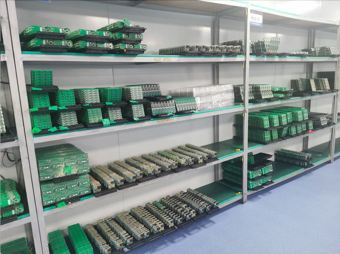
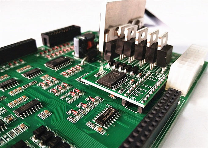
5.PCB Pictures