

| Place of Origin: | China |
|---|---|
| Brand Name: | Null |
| Certification: | ISO9001 | UL ( E337072 ) | TS16949 ( 0259279 ) | RoHS |
| Model Number: | Kingsum Electronic |
| Minimum Order Quantity: | 1pcs |
|---|---|
| Price: | 0.1-5 USD |
| Packaging Details: | Vacuum Package |
| Delivery Time: | 5 -8 days |
| Payment Terms: | T/T, Western Union, Paypal |
| Supply Ability: | 20000 meter |
| SMT And DIP: | Support | Application: | Camera PCBA |
|---|---|---|---|
| Components: | Supplied By Customers Or Supplied By Manufacturer | PCB Test: | AOI ; 100%test For Open And Short; |
| PCBA Test: | X-ray,Function Test | PCB: | HDI With Laser And Buried Holes |
| High Light: | HDI PCB Assembly Service,ENIG PCB Assembly Service,FR4 6 Layer Pcb Board | ||
1. Detailed Specifications
| Material | FR4 |
| Board Thickness | 1.6mm |
| Surface Treatment | ENIG+OSP |
| Copper Thickness | 1/1/1/1/1/1 OZ |
| Soldermask | Black |
| Silkscreen | White |
| The Min Laser Drill Hole | 4 Mill |
| Panel | Mouse Bite |
Introduction:
Printed Circuit Board Assembly it to plug the SMT(Surface Mounted Technolofy) and the DIP in the Printed Circuit Board, also called PCBA.
Production:
Both SMT and DIP are means of integrating components in the PCB board. The main difference is that SMT does not need to drill holes on the PCB,while it's nacessary for the DIP to plug the pin of the component into the drilled hole.
SMT:
Mainly use the paste to pack machine to attach some micro components the PCB board. The production process is as follows: the PCB board positioning, solder paste printing, paste and pack, return to the soldering stove, finally inspection.
With the development of science and technology,SMT can also be applied to some large-size components.
DIP:
Insert the componets to the PCB. It is used as a mean to integrate components cause the size is too large to paste and pack, or the manufacturer's production process cannot use SMT technology.
At present, there are two ways to realize manual plug-in and robot plug-in.
The main production processes are as follows: paste back glue (to prevent tin plating to inappropriate places), plug-in, inspection, wave soldering, brush plate (to remove the stain left in the process of passing the furnace) and inspection
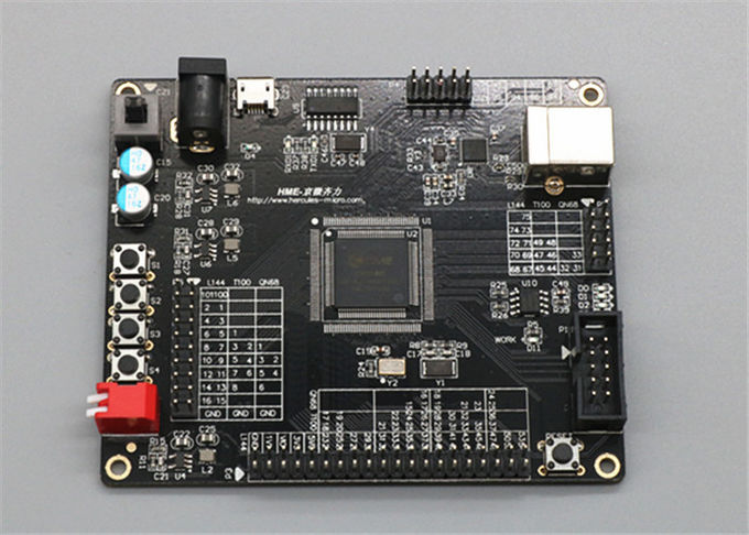
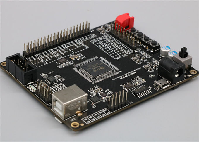
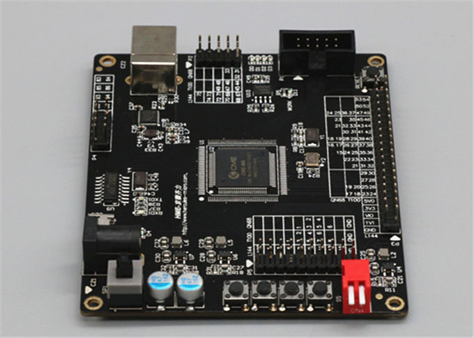
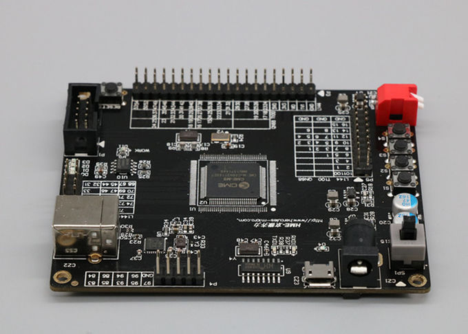
2. Pictures
FAQ
Q: What files do you use in PCB fabrication?
A: Gerber or Eagle, BOM listing, PNP and Components Position
Q:Is it possible you could offer sample?
A: Yes, we can custom you sample to test before mass production
Q: When will I get the quotation after sent Gerber, BOM and test procedure?
A: Within 6 hours for PCB quotation and around 24-48 hours for PCBA quotation.
Q: How can I know the process of my PCB production?
A: 5-7days for PCB production and components purchasing, and 14 days for PCB assembly and Testing.
Q: How can I make sure the quality of my PCB?
A: We ensure that each piece of PCB products work well before shipping. We'll test all of them according to your test procedure.


