


| Place of Origin: | China |
|---|---|
| Brand Name: | Null |
| Certification: | ISO9001 | UL ( E337072 ) | TS16949 ( 0259279 ) | RoHS |
| Model Number: | Kingsum Electronic |
| Minimum Order Quantity: | 1pcs |
|---|---|
| Price: | 0.1-5 USD |
| Packaging Details: | Vacuum Package |
| Delivery Time: | 5 -8 days |
| Payment Terms: | T/T, Western Union, Paypal |
| Supply Ability: | 20000 meter |
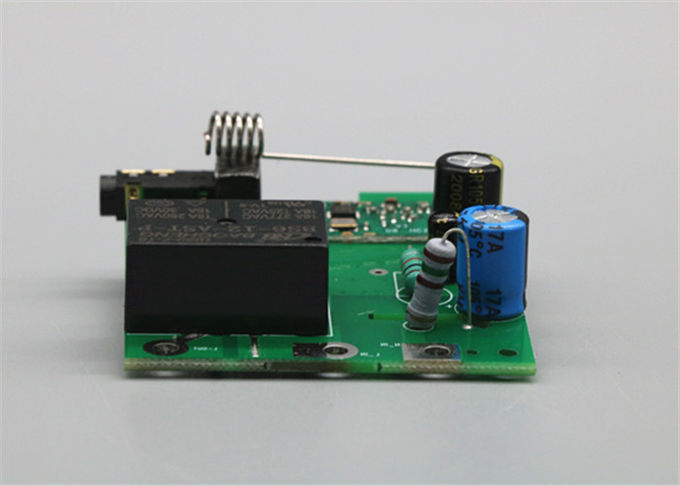
| SMT And DIP: | Support | Application: | Camera PCBA |
|---|---|---|---|
| Components: | Supplied By Customers Or Supplied By Manufacturer | PCB Test: | AOI ; 100%test For Open And Short; |
| PCBA Test: | X-ray,Function Test | PCB: | HDI With Laser And Buried Holes |
| High Light: | HDI Printed Circuit Board Assembly,ENIG Printed Circuit Board Assembly,OSP 6 Layer Prototype Assembly | ||
1. Detailed Specifications
| Material | FR4 |
| Board Thickness | 1.6mm |
| Surface Treatment | ENIG+OSP |
| Copper Thickness | 1/1/1/1/1/1 OZ |
| Soldermask | Green |
| Silkscreen | White |
| The Min Laser Drill Hole | 4 Mill |
| Panel | Mouse Bite |
Introduction:
Printed Circuit Board Assembly it to plug the SMT(Surface Mounted Technolofy) and the DIP in the Printed Circuit Board, also called PCBA.
Production:
Both SMT and DIP are means of integrating components in the PCB board. The main difference is that SMT does not need to drill holes on the PCB,while it's nacessary for the DIP to plug the pin of the component into the drilled hole.
SMT:
Mainly use the paste to pack machine to attach some micro components the PCB board. The production process is as follows: the PCB board positioning, solder paste printing, paste and pack, return to the soldering stove, finally inspection.
2. Pictures