
| 原产地: | 中国 |
|---|---|
| 品牌名称: | Kingsum Electronic |
| 认证: | UL-ROHS |
| 型号: | Kingsum ElectronicA-007 |
| 最小订单数量: | 1台 |
|---|---|
| 价格: | 0.1-20美元/台 |
| 包装细节: | P/P,纸箱 |
| 交货时间: | 10~20个工作日 |
| 付款条件: | 电汇、西联汇款、速汇金、信用证、承兑交单 |
| 供应能力: | 2000平方米/月 |
| Layer Count: | 2 ` 30 Layers | Max Board Size: | 600 Mm X 1200 Mm |
|---|---|---|---|
| Base Material For PCB: | FR4, CEM-1, TACONIC, Aluminium, High Tg Material, High Frequence ROGERS ,TEFLON, ARLON, Halogen-free Material | Rang Of Finish Baords Thickness: | 0.21-7.0mm |
| Minimum Line Width: | 3mil (0.075mm) | Minimum Line Space: | 3mil (0.075mm) |
| Minimum Hole Diameter: | 0.10 Mm | Finishing Treatment: | HASL (Tin-Lead Free), ENIG(Immersion Gold), Immersion Silver , Gold Plating (Flash Gold), OSP, Etc. |
| Thickness Of Copper: | 0.5-14oz (18-490um) | E-Testing: | 100% E-Testing (High Voltage Testing); Flying Probe Testing |
| High Light: | printed circuit board pcb,power supply circuit board | ||
1. Features of Camera PCBA
2. Camera PCBA Technical capability
| SMT | Position accuracy:20 um |
| Components size:0.4×0.2mm(01005) —130×79mm,Flip-CHIP,QFP,BGA,POP | |
| Max. component height::25mm | |
| Max. PCB size:680×500mm | |
| Min. PCB size:no limited | |
| PCB thickness:0.3 to 6mm | |
| PCB weight:3KG | |
| Wave-Solder | Max. PCB width:450mm |
| Min. PCB width: no limited | |
| Component height:Top 120mm/Bot 15mm | |
| Sweat-Solder | Metal type :part, whole, inlay, sidestep |
| Metal material:Copper , Aluminum | |
| Surface Finish:plating Au, plating sliver , plating Sn | |
| Air bladder rate:less than20% | |
| Press-fit | Press range:0-50KN |
| Max. PCB size:800X600mm | |
| Testing | ICT,Probe flying,burn-in,function test,temperature cycling |
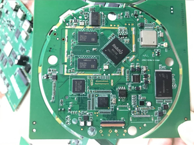
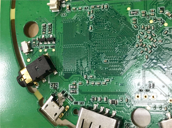
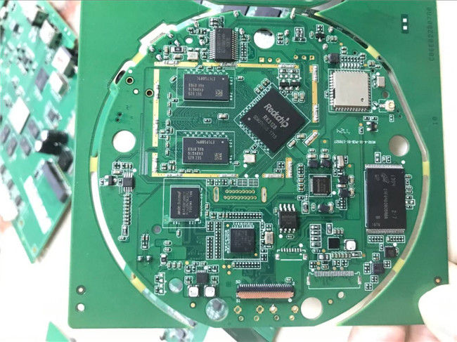
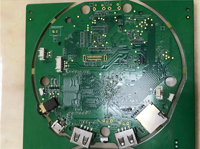
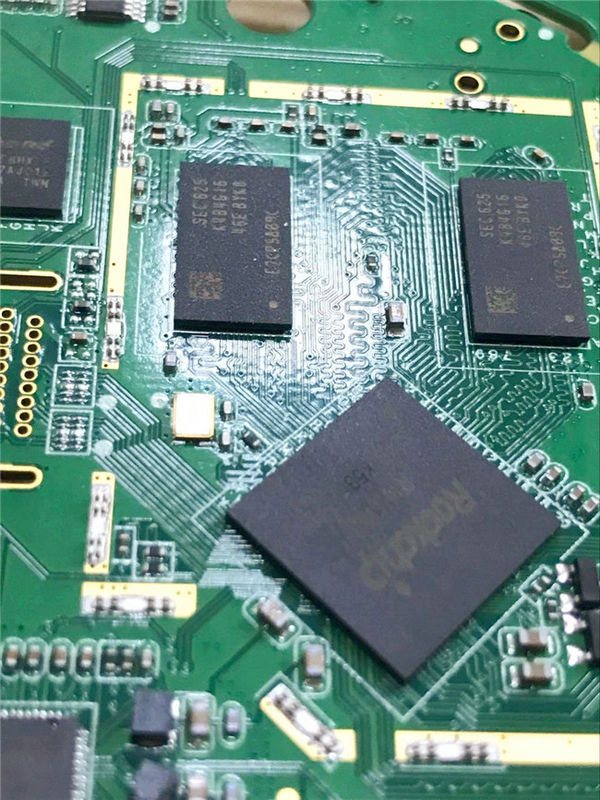
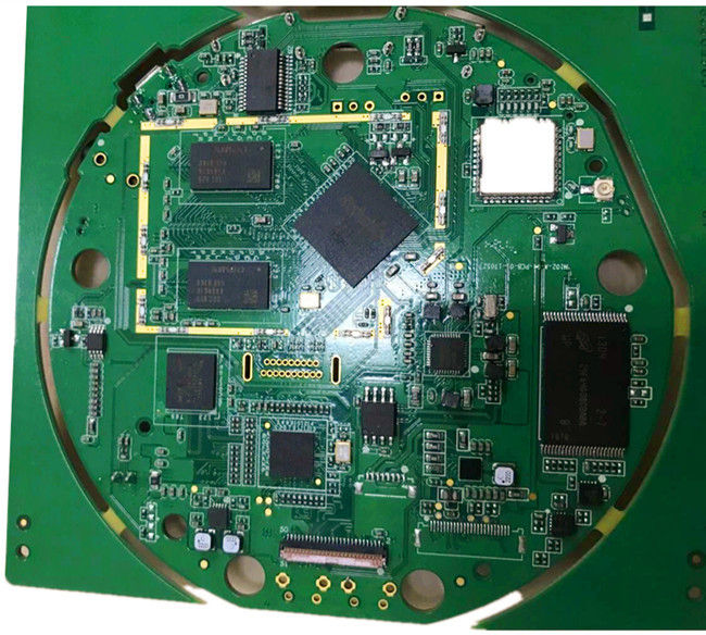
3. Camera PCBA Pictures