


| Place of Origin: | China |
|---|---|
| Brand Name: | OEM ODM |
| Certification: | ISO9001, TS16949, UL, RoHS |
| Model Number: | PCBA-J-69 |
| Minimum Order Quantity: | 1 pc |
|---|---|
| Price: | USD/pc |
| Packaging Details: | Bubble Wrap |
| Delivery Time: | 2~3 weeks |
| Payment Terms: | T/T, Western Union, Paypal |
| Supply Ability: | 20,000 Square Meters / Month |
| Categary: | SMT PCBA Assembly | Material: | FR-4 |
|---|---|---|---|
| Layers: | 2-6 Layers | Board Thickness: | 1.6mm |
| Copper: | 1oz | Surface: | ENIG |
| Soldmask: | Green | Silk Screen: | White |
| Standard Testing: | IPC Class 2 | Used For Products: | ODM Products |
| High Light: | circuit board design,pcb board design | ||
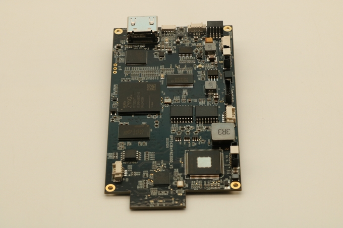
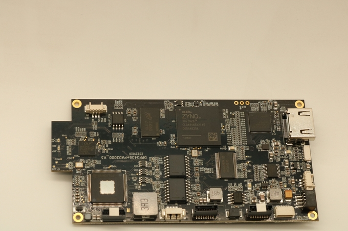
2-6Layers PCB ENIG/HASL PCB Design for customer requirements ODM Service
Detail Specifications:
| Layers | 2-6 |
| Material | FR-4 |
| Board Thickness | 1.6mm |
| Copper Thickness | 1oz |
| Surface Treatment | ENIG |
| Soldmask & Silkscreen | Green & White |
| Quality Standard | IPC Class 2, 100% E-testing |
| Certificates | TS16949, ISO9001, UL, RoHS |
Photoes of this 2-6Layers PCB ENIG/HASL PCB Design for customer requirements ODM Service
What KAZ Circuit can do for you:
To get a full quotation of the PCB/PCBA, pls provide the information as below:
Company Informaiton:
KAZ Circuit is a professional PCB manufacturer from China since 2007, also provide PCB Assembly service for our customers. Now with about 300 employees. Certified with ISO9001,TS16949, UL, RoHS. We are confident to provide you quality products with factory-directed price within the fastest delivery time!
Manufacturer Capacity:
| Capacity |
Double Sided: 12000 sq.m / month Multilayers: 8000sq.m / month |
| Min Line Width/Gap | 4/4 mil (1mil=0.0254mm) |
| Board Thickness | 0.3~4.0mm |
| Layers | 1~20 layers |
| Material | FR-4, Aluminum, PI |
| Copper Thickness | 0.5~4oz |
| Material Tg | Tg140~Tg170 |
| Max PCB Size | 600*1200mm |
| Min Hole Size | 0.2mm (+/- 0.025) |
| Surface Treatment | HASL, ENIG, OSP |


